Main Page/PHYS 3220/Semiconductors I
Contents
Semiconductors I
Introduction
In this experiment we perform measurements on two differently doped samples of germanium to explore the conduction mechanisms in semiconductors. First the resistivity of the material is investigated by means of the current-voltage characteristic at room temperature. Next resistivity, at fixed current, is explored as a function of temperature in the range of -5 to 100 º C. In the third part the Hall effect is investigated by placing the semiconductor bar into a magnetic field.
Many references on solid-state physics exist that deal with the problem of conduction mechanisms in doped semiconductors. A good introduction to the physics needed for this experiment is given by A. Melissinos (ref. 1, chapter 3). A few of the essential concepts are reviewed in this introduction.
To understand the temperature dependence of the resistivity you must understand that two conduction mechanisms are in operation in the different temperature ranges. A perfect (pure) germanium crystal acts as an insulator. Natural impurities turn it into a poor conductor. To control the conduction process one adds impurities of a certain type. Elements with three outer electrons when added to the germanium provide hole states inside the gap near the valence band. These are excited even at low temperatures and populate the conduction band. Elements with five outer electrons also bind into the germanium crystal and easily give up their surplus electron, i.e., provide electron states close to the conduction band. One refers to the semiconductor material as being p-type or n-type doped respectively.
At low temperatures extrinsic conduction works, which is the result of impurities in the germanium providing electron and hole carriers. Above liquid nitrogen temperatures the impurity levels are all excited, i.e., saturated and an increase in temperature does not lead to an increase in transfer of these electron states to the conduction band (hole states to the valence band). Below room temperature there is only a small number of intrinsic charge carriers, i.e., transfers of valence electrons to the conduction band, since the energy gap is relatively large (about 0.7 eV; recall that at room temperature kT ≈ 0.025 eV). For high enough temperatures such that the intrinsic charge carrier mechanism dominates (but nevertheless a low-temperature approximation to the Fermi distribution is still valid) the charge carrier density dependence on temperature is given by
 | (1) |
This expression can be used to express the resistivity (or voltage at constant bias current) as a function of temperature. The result will be different for both samples, since it also depends on the amount of charge carriers available. The additional quantities of interest to understand conduction are the mobility µ (defined as the proportionality constant between the average drift velocity and the applied electric field µE = vd); the conductivity (inverse of resistivity ρ) σ = 1/ρ, which relates the applied field and the current density J = σE. The conductivity is proportional to the charge carrier mobility and density (and the electron charge e): σ = n e µ . Resistivity and resistance R are related via the cross-sectional area A and the length of the sample l as ρ = R A l-1. To observe the Hall effect one places the semiconductor material into a magnetic field and measures how the Lorentz force deflects the charge carriers in a direction perpendicular to the field and the current (a voltage VH arises). This allows one to deduce not only the amount of charge carriers (at fixed T), but also which type dominates the conduction mechanism. The Hall coefficient is defined for given magnetic field strength B and generated electric Hall field Ey as
 | (2) |
It provides a measure of the density of the charge carriers, since the Lorentz force depends on the drift velocity. Equating the compensating Hall field to the magnitude of the magnetic force allows us to relate the magnitude of RH to the inverse of the carrier density.
Experimental Procedure
Apparatus
Sample and Holder
Two semiconductor samples designated RCA A and RCA B are supplied consisting of two bars of germanium (one n-type, one p-type material) mounted at the base of metal tubes. Figure 1 shows the location and function of the six contacts made to each of the samples. The samples and connections to them are visible through the plastic coating applied to protect the contacts. Understand the function of the contacts as explained in Fig. 1 and observe how the connections are realized on the two samples (contact 1 is on the sample holder side; Fig. 2 provides an explanation of current direction [engineer’s convention!] for given position of the current reversing switch on the bias supply unit).
 Figure 1 - Contacts to the germanium samples.
|
| Contacts | Dimensions | |
| (1,2) Bias Current | t = 0.11 ± .005 cm | |
| VR | (3,4) Resistivity measurements | w = 0.11 ± .005 cm |
| VH | (5,6) Hall voltage measurements | x = 0.6 ± .01 cm |
 Figure 2 - Current direction through sample for + and – positions on bias supply unit.
|
Leads from the germanium sample are connected to via a six-conductor cable terminating in a six-pin Jones' plug. The fragile leads to the germanium bars are potted in epoxy to prevent accidental damage to the connections. The top surfaces of the samples are left exposed to permit measurements of the thermo-electric effect, and to provide close proximity to the bulb of the thermometer. The thermometer (range -20ºC to 150ºC) is used to measure the temperature of the sample and care should be taken to ensure that the bulb is close to the sample during measurements. The range of temperatures used in the experiments is obtained in two stages. The lower range -5ºC to 20ºC is achieved using a mixture of glycol (antifreeze) and dry ice. The 20ºC to 120ºC range is obtained by heating the glycol solution using a hot plate with magnetic mixer.
Current Bias Supply
The current supply to the sample may be varied from 0 to 1 mA by turning the control knob labelled 0-1 mA located on the front panel. This adjusts a potentiometer connected across two 9V batteries. The current passing through the germanium bar is measured by the milliammeter located on the front panel. The circuit diagram for the current supply is shown in Fig. 3.
The direction of the current through the germanium bar can be reversed using the reversing switch (marked " + OFF -") on the front panel. The germanium sample is connected to the bias supply by inserting the Jones' plug, terminating the cable leading from the sample, into the socket at the side of the current biasing unit. The two pairs of outlets, labelled VR and VH, provide access to the appropriate contacts on the sample (see Fig. 1) to permit measurements of the voltages arising on the sample. The white outlet is the common ground connection for the system and must be connected to the white outlet on the voltmeter whenever voltage measurements are being made.
 Figure 3 - Current bias supply circuit diagram.
|
Note:To preserve the life of the battery, the reversing switch should always be in the central "OFF" position when measurements are not being made. If, during the course of the experiments, difficulty is encountered achieving the maximum bias current (1 mA), the batteries must be replaced.
Voltmeter and Amplifier Unit
The voltmeter contains amplifying circuits which allow us to measure the voltages along and across the germanium samples. The circuits diagram is shown in Fig. 4. The circuit contains an integrated-circuit operational amplifier (OpAmp) that produces gains which enable the output meter (500 μA) to measure voltages in the range 0 to 200 millivolts (resistivity experiments) or 0 to 2 millivolts (Hall effect experiments). Observe from the circuit diagram how the selection of the appropriate position, VR or VH respectively (using the selector switch on the front panel) changes the gain factor of the OpAmp (by choosing different resistors). An additional push-button switch is provided to increase the sensitivity by a factor 2 on either setting. An offset voltage, controlled by the offset potentiometer (see Fig. 4), is required to adjust the zero point of the amplifier. The operating voltages (positive and negative against ground) are supplied by two 9 Volt batteries.
 Figure 4 - Circuit Diagram of the Voltmeter and Amplifier Unit.
|
Battery Check
Before each experiment, the batteries should be checked for both units. For the measuring unit this is performed using the 3 coloured sockets on the left hand side as follows:
- Connect a digital voltmeter to the red and white sockets on the left side of the unit.
- Check that the reading on the voltmeter is greater than 8 Volts (9V batteries, particularly non-alkaline types, deliver voltages lower than 8V when they are nearly exhausted).
- Change the leads from the positive and negative terminals of the voltmeter to the white and black sockets respectively.
- Check that the voltmeter reading is greater than 8 Volts. Replace batteries as necessary.
Measurement of Resistivity
Tasks
- Determine the relationship between the voltage, VR, arising across the two contacts, 3 and 4, on the sides of each of the semiconductor samples A and B and the current I passing through the bars (through contacts 1 and 2).
- Calculate from the data the resistivities of the two semiconductor samples A and B at room temperature (with error analysis).
- Calculate the charge carrier concentration in the two samples from the measured resistivity using standard values for the mobilities in n-type and p-type germanium.
Apparatus
- Two germanium samples, RCA A and RCA B.
- RCA current bias supply unit and leads.
- RCA voltmeter and amplifier unit.
- digital voltmeter.
Procedure
- Connect the white sockets (terminals marked: 2) of both the measuring and the current bias supply units using the white wire. This provides the units with a common ground.
- Connect terminals 3 and 4 (VR) on the current bias supply unit to the VR terminals (3 and 4) on the measuring unit using the yellow and green leads (connecting likewise colours).
- Ensure that the current bias supply unit is set to the "OFF" position. When connecting a semiconductor to a circuit never use leads that are ‘live’, since the transistor, diode, etc. , may easily be damaged otherwise. Connect the sample (RCA A) to the current bias supply unit by inserting the Jones' plug, terminating the wires leading from the sample, into the socket on the left hand side of the unit.
- Set the selector switch on the front of the voltmeter and amplifier unit (marked VH - OFF - VR) to the VR position. This sets the voltage scale to read a maximum of ± 200 millivolts.
Contacts 3 and 4 on the sample are now connected to the inputs of the OpAmp (via 10kΩ and 100Ω resistors), while contacts 1 and 2 are connected to the bias supply unit. A modest gain of 3 is obtained from the amplifier for the chosen resistor values.
Measurments
- Adjust the offset voltage potentiometer on the front panel of the voltmeter and amplifier unit until the voltmeter reading is zero.
- Set the current reversing switch (marked + OFF -) on the bias supply to +. The current now flows through the germanium sample as indicated in Fig. 2.
- Measure the voltage VR, on the voltmeter (a digital voltmeter should be attached to the measuring unit), for various bias currents, I, at 0.2 milliampere intervals. The bias current is adjusted via the control knob (marked 0 - 1 mA) on the supply unit.
- Tabulate the results.
Before removing or inserting the Jones' plug leading from the samples into the socket of the current bias supply, set the reversing switch on the current bias supply unit and the selector switch on the voltmeter and amplifier unit to the OFF position.
- Repeat steps a) through d) for the sample RCA B.
- Plot VR versus I on a linear graph for both samples A and B. Take additional readings, if the slope is not readily determined from the number of readings taken. Obtain the resistance (and resistivity) using a linear fit for samples A and B.
Questions
- Does the resistance vary with the bias current (within the range measured)?
- How does the VR - I characteristic change if the bias is reversed? Confirm the prediction by reversing the polarity switch marked (-OFF +) to -, and repeating the experiment for one of the samples.
- Calculate the resistivity of the two germanium samples. The dimensions of the samples and the distance "x" are given in figure 1. If the resistivities of the two samples are different, how can you account for this? How does the resistivity compare to that of metals (e.g. copper)?
- From your experimental results, what do you conclude about the two samples RCA A, and RCA B?
- Calculate the carrier concentrations of the two germanium samples assuming the mobilities of the carriers in samples A and B at room temperature are given as 3600 and 1800 cm2/Volt-sec. respectively (ref. 2).
Variation of Resistivity with Temperature
Tasks
- Determine the relationship between resistivity and temperature for two bars of germanium in the temperature range -5ºC to 120ºC.
- Analyze and explain the relationship obtained between resistivity and temperature.
- Calculate the energy gap (ΔE) between the valence energy band and the lowest conduction energy band in the two germanium samples.
Apparatus
- Two germanium samples RCA A and RCA B.
- Thermometer -20ºC to 150ºC.
- RCA current bias supply unit and leads.
- RCA voltmeter and amplifier unit; digital voltmeter.
- 250 ml glass beaker
- Dry ice (solid carbon dioxide)
- Retort stand and clamps
- Glycol solution (automobile anti-freeze)
- Hot plate with magnetic stirring device
Procedure
- Follow procedures 1 through 4 from the previous section.
- Place the thermometer in the sample holder and secure it. The bulb of the thermometer must be placed as close to the germanium sample as possible.
- Fill the glass beaker 2/3 full of glycol solution. Insert the germanium sample into the glycol solution such that it is midway between the bottom of the beaker and the surface of the glycol and in the centre of the beaker. Secure the sample in this position with a retort stand and clamps. No significant length of the metal sample holder should be dipping into the glycol, since metals are good conductors and create temperature gradients in the liquid.
Measurements
- Adjust the offset voltage potentiometer on the front panel of the voltmeter and amplifier until the voltmeter reading is zero.
- Set the reversing switch (marked "+ OFF -") on the current bias supply to +. (cf. fig 2).
- Adjust the knob designated 0 - 1 mA on the bias supply so that about 0.5 mA passes through the sample as observed on the milliammeter.
- Add some dry ice to the glycol solution. Stir until the temperature falls to -5ºC.
- Keep the bias current constant at 0.5 mA, and measure the voltage VR as the sample warms up. Take readings at 5ºC intervals from -5ºC to 20ºC.
- Heat the glycol solution using the hot plate until a temperature of 120ºC is reached. Take care not to exceed 125ºC or the soldered connections to the germanium bar may be damaged.
- Keeping the current constant, measure the voltage VR at 5ºC intervals as the sample cools from 120ºC to 25ºC. Stir the solution continuously to ensure a uniform temperature. If the cooling process is too slow below 50ºC, add small quantities of dry ice to the warm glycol solution to reduce the temperature at a faster rate.
- Tabulate the voltage VR versus T.
- Repeat the experiment with the second germanium sample (RCA B) in the temperature range 120ºC to 25ºC. Make sure that the reversing switch on the bias supply and the selector switch on the voltmeter are in the "OFF" positions when changing the samples.
- Plot graphs of loge VR versus the reciprocal of absolute temperature T [ºK] on a linear scale.
Questions
- Inspect the graph obtained in step (j). For what region is equation (1) valid?
- Determine the energy gap (ΔE) for the germanium bar.
- Discuss why equation (1) is not valid for all T. Compare the findings with ref. 1.
- What are the sources of error? How could the experimental procedure be improved? What is the error in your estimate of the energy gap ΔE for germanium? How does it compare with literature values (see e.g., ref. 2)?
Measurement of the Hall Voltage
Tasks
- Determine the relationship between the Hall voltage and the bias current for a germanium sample placed in a known magnetic field.
- Calculate the Hall coefficient, charge carrier concentration, and the mobility of the carriers in p-type and n-type germanium.
Apparatus
- Two germanium sample RCA A and RCA B.
- RCA current bias supply unit and leads.
- RCA voltmeter and amplifier unit; digital voltmeter.
- Permanent magnet and soft iron spacers.
Procedure
- Using a white lead, connect the white socket (terminals marked 2) of the measuring and the current bias supply units. This provides the units with a common ground.
- Connect terminals 5 and 6 (VH) and the current bias supply unit to the VH terminals (5 and 6) on the measuring unit using the red and black leads, connecting likewise colours. Remove the VR connections if these are still present from a previous experiment!
- Ensure that the current bias supply is switched to the "OFF" position. Connect the sample (RCA A) to the current bias supply unit by inserting the Jones' plug.
Set the selector switch on the front of the voltmeter and amplifier (marked VH -OFF- VR) to the VH position. The voltmeter is now set to the ± 2 millivolts range. Inspect the connections as per figs. 1 and 2. Contacts 5 and 6 are now connected with the OpAmp inputs via the 100Ω resistors (a gain of 300 is obtained by the amplifier).
CHECK that the cables connecting the two units are connecting the VH terminals (5 and 6 respectively). Mixing the connection will give wrong results and may damage the voltmeter.
- Adjust the offset potentiometer on the front panel of the voltmeter and amplifier unit to obtain a zero reading on the voltmeter.
Measurements
- Set the reversing switch on the current bias supply unit to +. This makes the current flow through the sample in the direction shown in Fig. 2.
- Adjust the control knob (marked 0-1 mA) on the current bias supply unit to give a current reading of 0.2 mA, on the milliammeter.
- Adjust the offset voltage potentiometer to obtain a zero reading. This provides the necessary offset voltage for the amplifier operation, and also compensates for any voltage arising between terminals 5 and 6 on the sample. The latter can be caused by the contacts 5 and 6 not being exactly opposite from each other.
- Take off your wristwatch and place it away from the magnet. Remove the iron keeper from between the pole pieces of the magnet. Attach the two soft iron spacers provided, one to each pole of the magnet, by sliding them along the top of the magnet and down into position over the pole pieces. When the experiment is completed, remove the soft iron spacers and replace the keeper in position. This preserves the magnet. (Optional: Measure the magnetic field using a Gaussmeter).
- Place the sample (RCA A) between the pole pieces of the magnet so that it is central and equidistant from the poles. Record the sign and the magnitude of the voltage VH.
- Remove the sample from the magnet, rotate it by 180º, and repeat step (e). See Fig. 5.
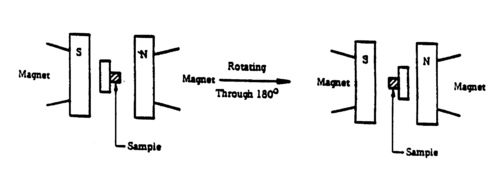
Figure 5 - Orientation of the sample between magnet poles.
- Remove the sample from the magnet. Set the reversing switch on the current bias supply unit to the "-" position. Adjust the voltmeter for zero reading. Perform steps (e) and (f).
- Repeat steps b) through g) for different bias currents using 0.2mA steps (0.2, 0.4, 0.6, 0.8 and 1mA).
- Tabulate the measured Hall voltages VH versus positive and negative bias current for both positions.
- Repeat the experiment (items a through i) with the other sample (RCA B). Take care to switch off all voltages when changing the samples.
- Plot the Hall voltages VH versus bias current for both germanium bars on a linear scale. Take the average of the magnitudes of the four Hall voltage readings obtained for each current setting.

Questions
- Taking into account the direction of the current bias, the applied magnetic field, and the measured Hall voltage, determine the charge sign of the majority carrier for samples A and B (cf.. Fig. 2).
- From your data (Hall voltage, bias current, magnetic field and sample dimensions) calculate the Hall coefficients, RA and RB for the two samples (eq. 2). Calculate the majority carrier concentrations for each sample. Compare these results with the carrier concentrations obtained from your conductivity measurements and comment.
- Calculate the carrier mobility in the Hall Field for each of the samples. Compare your results with those quoted at the end of section 2.1.
- Can you account for the errors in the derived values?
Consider:
- Meter accuracy and meter reading accuracy.
- Quoted magnetic flux density.
- Sample dimensions.
- Suggest a practical application for a germanium Hall voltage sample such as you have used in this experiment.
- If a sample of "intrinsic" germanium is used to replace samples A and B, how will it behave in the above experiments?
References
- A.C. Melissinos, Experiments in Modern Physics.
- C. Kittel, Solid State Physics.