Main Page/PHYS 4210/Semiconductors II
Contents
Semiconductors II
Introduction
This laboratory extends your understanding of semiconductors from the first part, where the conduction mechanism in a single-zone doped sample of germanium was investigated, to the so-called p-n junction. This junction forms the basis of semiconductor switching and amplification devices. A diode consists of a single p-n junction, while a simple transistor contains three zones assembled either as p-n-p, or n-p-n.
The concepts of charge carrier injection and excess carriers are introduced. Furthermore, the difference between ohmic and rectifying contacts is demonstrated, and the terms ‘emitter’ and ‘collector’ are explained. Experiments on the detection of carriers at the collector demonstrate the existence of excess carriers generated both by injection and optical methods. Measurements are made that allow us to calculate the mobility of these carriers, and a further experiment provides an estimate of their lifetime.
The physics of the p-n junction is explained in most textbooks on modern physics. Simple presentations are given, e.g., in refs. 1,2, which explain how the current-voltage characteristic of a diode (p-n junction) arises:
| (1) |
Make sure to understand the electric fields (and the potential) that arise across the three zones (pure p, pure n, and the depletion region that joins the two) and give rise together with the Maxwell-Boltzmann distribution for the charge carrier diffusion process to eq. (1).
The laboratory consists of three experiments:
- Investigation of the difference between ohmic and rectifying contacts. Measurement of the current-voltage characteristic.
- Verification of the existence of minority carriers created by injection. Measurement of the minority carrier mobility.
- Generation of minority carriers by optical means. Measurement of the minority carrier lifetime.
Experimental Procedure
The Apparatus
The Sample and Holder
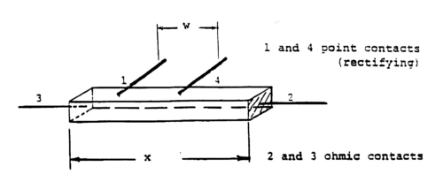
The n-type germanium sample, ready prepared with suitable contacts, is mounted on a printed circuit board and potted in a clear plastic compound. The sample and connections are visible and at the same time are protected from external hazards. The connections to the sample are shown in Fig. 1.
|
Figure 1 - Contacts to the germanium sample.
|
Contacts 2 and 3, applied to the ends of the bar, are ohmic. Contacts 1 and 4 are "point" contacts, made in such a way as to permit the generation and collection of minority carriers. The four leads from these contacts terminate in a four-pin Jones plug that inserts into the matching socket of the bias supply unit. The two holes in the sample mounting board enable the germanium sample to be mounted on the manipulator. It is recommended that the sample be retained in this position throughout the experiments to reduce any unnecessary stress on the cable.
The Manipulator
The manipulator, which is held by two screws to the front panel of the bias supply box, provides a means of moving the sample through a distance of approximately 15 mm. This is required for the minority carrier lifetime measurements. One complete turn of the screw moves the sample through 0.5 mm.
The Light Source
The light source consists of a 6.5 Volt, 2.75 A, pre-focussed lamp, installed in a housing along with a lens system which produces an intense spot of light. A cover with a small aperture is supplied, and this is suitably placed over the sample so that only a very small pinpoint of light falls on a particular part of the sample. The position of the sample can then be adjusted using the manipulator. The light source plugs into the two-pin socket on the side of the bias supply that, in turn, is connected to a transformer inside the box providing the required current and voltage. An on-off switch, adjacent to the socket, operates the light.
The Current Bias Supply and Pulse Generator
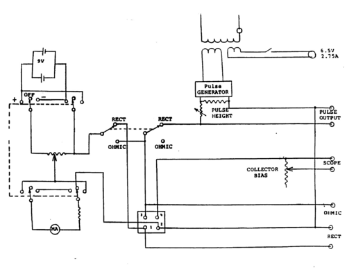
The DC current bias required for the various experiments is supplied from two 9 V batteries. A potentiometer, connected across the batteries, provides a continuously variable current from 0-1 mA, which is monitored on the milliammeter located on the front panel. The milliammeter is located on the front panel. The milliammeter is provided with an internal shunt that enables the meter to record either 0-100 μA or 0-1 mA, by selecting the appropriate range using the range selector switch below the meter. The current direction can be reversed using the reversing switch marked (+ OFF - ) on the front panel. The current passes through the germanium sample either through contacts 1 and 2 or through 3 and 2 depending on whether the contact switch on the front panel is set at "RECT" or "OHMIC" respectively. The voltage arising across the pairs of contacts 1 and 2 or 3 and 2 can be measured by connecting a voltmeter to the outlets of the supply unit, marked "OHMIC" or "RECT".
|
Figure 2 - Bias Supply and Pulse Generator Circuit Diagram.
|
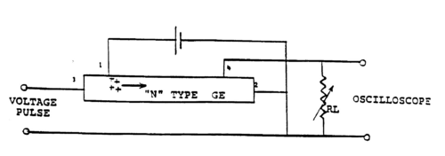
A pulse generator is incorporated in the supply unit. It is produces a positive square pulse of approximately 100 msec with a repetition rate of approximately 10 milliseconds. The pulse height can be adjusted continuously from 20 to 40 Volts into a 200 Ω load (typical resistance of a germanium sample). The switch and potentiometer controlling the pulse generator, which operates from a 115 V, 60 Hz supply, are located on the front panel to the right of the meter. The supply is protected with a 0.5 A fuse situated at the side of the box. With the contact switch in the "RECT" position, the pulse output is fed internally to contacts 3 and 2 of the sample via a four-pin Jones plug. The pulse height can be measured by connecting the oscilloscope to the outlets labelled "pulse output" on the front panel.
Applying a positive pulse across contacts 3 and 2 of the sample causes the point contact numbered 4 on the sample to become reverse biased and a small reverse current will flow between it and contact 2. This current is measured by connecting the oscilloscope to the outlet labelled "oscilloscope" and observing the voltage arising across a 50 KΩ variable resistor labelled "collector bias" in series with the point contact 4. Adjusting the "collector bias" varies the reverse voltage applied to the point contact. The circuit diagram for the bias supply, pulse generator and sample is shown in Fig. 2.
Note: To install or replace a battery, disconnect the sample and remove the two screws at the front of the cabinet. The whole of the front panel of the cabinet then swings up, clearly exposing the battery holder and its connections.
Ohmic and Rectifying Contacts
Contacts between a metal and a semiconductor, or between two semiconductors, play an important role in the operation of semiconductor devices. Two types of contacts are known:
- ohmic contacts, for which the current-voltage characteristic is symmetrical and obey Ohm's law;
- rectifying contacts, for which the current flows more easily in one direction.
Ohmic contacts can be difficult to achieve in practice, particularly when making contacts with pure semiconductor material.
Apparatus
- N-type germanium sample with two point contacts
- Current bias supply
- Multirange voltmeter
Procedure
- Connect the sample to the four-pin socket on the side of the supply unit. Switch the contact switch to "OHMIC". This permits the current to flow through the two ohmic contacts 2 and 3 at the ends of the sample. (See Fig. 1).
- Set the current switch to '+' and connect the multi-range voltmeter across the orange and black sockets marked "OHMIC" on the supply unit.
- Select a suitable range on the ammeter and voltmeter and take a series of readings of millivolts for various currents in the 0 - 1 mA range.
- Turn down the bias to zero, switch the current to '-' and repeat the experiment.
- Set the contact switch to "RECT". This permits the current to flow through the point contact or rectifying contact 1 and the ohmic contact 2 on the germanium sample (See Fig. 1). Connect the multi-range voltmeter across the green and black terminals marked 'RECT' on the unit.
- Repeat steps (d) and (e) taking a series of voltage readings in the range 0-1 mA for current in the '+' direction in steps of 100 mA.
Turn the bias down to zero and switch to '-'. Repeat steps (d) and (e) taking a series of current readings for the voltage range 0-3V.
NOTE 1: Do not exceed 3 Volts as breakdown may occur which can permanently affect the characteristics of the point contact.
NOTE 2: If the multi-range voltmeter used has low input impedance then the meter itself can contribute an influence over the readings. Corrections can be made by repeating the experiment, without the sample, using the same meter ranges and by making the necessary adjustments to the first set of readings.
- Plot a graph of voltage versus current on a linear scale, for readings obtained with the contact switch in the "OHMIC" position.
- Plot a graph of current versus voltage on a log/linear scale for readings obtained with the contact switch in the "RECT" position.
Questions
- Use the observed current-voltage characteristics to comment on the type of contacts.
- Explain the behaviour obtained for rectifying contacts; refer to equation (1).
- How does the slope in the forward direction compare with the theoretical value?
- Discuss any deviations from the linear portion of the graph. Estimate the saturation current of this ‘diode’ from both the forward and reverse characteristics. Discuss the difference between ohmic and rectifying contacts.
- What can we learn about minority carrier injection from this experiment?
Drift Mobility of Minority Carriers in a Semiconductor
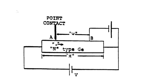
The previous experiment led us to conclude that excess carriers can be injected into a semiconductor by forward biasing a rectifying point contact. Consider a bar of n-type geranium into which minority carriers (holes) are injected at a point contact A. (See Fig. 3).
|
Figure 3 - Germanium bar with point contact.
|
If a voltage V is applied across the ends of the bar, then the holes will drift along the bar towards the negative contact with an average velocity proportional to the applied electric field. If a rectifying contact is placed at point B and is reverse biased, then the electric field set up at B will be such as to attract the holes as they pass, enabling them to be collected and detected.
It is important to note that the holes will only be detected at B if the time taken to travel from A to B is considerably less than the average lifetime of the injected carriers.
The average drift velocity of the minority carriers v (cm/sec) is given by
| (2) |
where μh is the mobility of the holes (cm2/volt sec.) and E is the applied electric field (volts/cm) given by E = V/x, where x is the length of the bar.
If w is the distance between A and B and t is the time taken for the carriers to move from A and B then:
| (3) |
or,
| (4) |
Apparatus
- N-type germanium with two point contacts.
- Bias supply and Pulse generator.
- Oscilloscope. (sensitivity 20 mV/cm vertical, 5μsec/cm horizontal).
This experiment can be performed in several ways, the two most common being (a) applying a dc drift field across the sample and injecting a pulse of excess carriers, or (b) continuous dc injection and a pulsed drift field. We use the second method to avoid heat dissipation problems. A simplified circuit diagram is shown in Fig. 4.
|
Figure 4 - Circuit diagram.
|
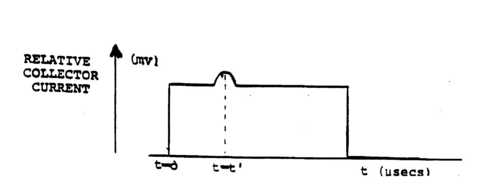
The contacts 2 and 3 at the ends of the n-type germanium bar are ohmic. The two point contacts 1 and 4 are located along the length of the bar, a few millimeters apart. Minority carriers (holes) are injected by forward biasing the emitter point contact 1. A voltage pulse can then be applied across the ends of the bar in such a way that points 1 and 4 become reverse biased. Consequently, minority carrier injection at contact 1 is cut off and the holes surrounding the point contact 1 are swept along the bar, under the influence of the pulsed drift field, past point 4 where collection occurs. The pulsed drift field must be of sufficient magnitude and duration to allow the holes to travel from the emitter contact 1 to collector contact 4. The collection is detected by connecting an oscilloscope across a series resistance RL in the collector circuit: the oscilloscope measures the collector current. A typical oscilloscope trace is shown in Fig. 5.
|
Figure 5 - Oscilloscope display.t = o is the time at which the pulsed field is applied
[ t' = time of arrival of the carriers at 4.]
|
Procedure
- Connect the germanium sample to the bias supply unit via the four-pin socket on the side of the box.
- Connect the oscilloscope to the sample using the read and black sockets marked "oscilloscope". Suitable settings are 5 μsecs/cm vertical.
- Turn the contact switch on the supply unit to "RECT" and the current bias switch to '+'. Positive bias can now be applied to the emitter point contact 1.
- Switch on the pulse generator and adjust the pulse height to produce an output pulse of about 25 Volts. (This is measured by connecting the oscilloscope to the red and black sockets; marked "PULSE OUTPUT" on the supply unit. A dual input oscilloscope is extremely convenient for this experiment since this will eliminate the necessity of having constantly to interchange connection).
- Adjust the "collector bias" so that the waveshape obtained on the oscilloscope has as square a leading edge as possible. This waveshape is a representation of the current in the collector circuit. Adjusting the "collector bias" alters the reverse voltage applied to the collector, which will alter the reverse current in this circuit.
- Adjust the bias control to give a symmetrical pulse superimposed on the rectangular waveshape. A typical current bias for the emitter is 1.0 milliamp. Excessive bias will produce over injection and give rise to an asymmetrical pulse. A typical waveshape is shown in Fig. 5.
- Take a series of readings of t' (microseconds), the time taken for the injected carriers to reach the collector, for different pulse height voltage V from 20 to 40 volts. Adjust the collector current bias when necessary for a satisfactory waveshape.
- Measure the distance between the emitter and collector (point contact 1 and 4) and the overall length of the germanium bar, between contacts 2 and 3.
- Plot the pulse height voltage V versus the reciprocal of time 1/t' on linear graph paper.
- From the graph calculate the mobility μh of the minority carriers. Use equation (7), and estimate the errors in the value of mobility μh.
- Compare the value of mobility μh with the literature value for the mobility of holes in germanium.
Questions
- Discuss the meaning of the terms emitter and collector as they apply to this experiment.
- What factors affect the number of carriers arriving at the collector? What limits can you place on the lifetime of the minority carriers?
- Is it possible to use p-type germanium for the above experiments? Discuss the required changes in the circuit.
Generation of Excess Carriers using Light
One of the most common methods of creating excess carriers in a semiconductor involves optical techniques. Photons striking a semiconductor will either be reflected at the front surface, absorbed within the bulk, or transmitted through the material. Photons absorbed in the material will lose their energy either by generating electron-hole pairs, or by giving up energy to the germanium lattice.
If electron-hole pairs are generated, then an increase in the number of majority and minority carriers will be expected. The conductivity of the material will be increased. This process of electron-hole generation by light is called photoconductivity, and for this to occur, the incident photon must have an energy greater than the energy band-gap of the semiconductor material in question. The energy of a photon is given by E = hc/λ where h = Planck's constant (6.6 x 10⁻³⁴ joule sec), c is the velocity of light (3 x 1010 cm/sec) and λ is the wavelength of the photons. Taking the band-gap for germanium to be 0.66eV, it can be seen that photons having a wavelength less than 1.8 microns will contribute to the photoconduction process.
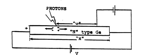
If we now consider a bar of n-type germanium and shine light of a suitable wavelength on the bar, electron-hole pairs will be generated, see Fig. 6.
|
Figure 6 - Circuit diagram.
|
If the electron-hole pairs are generated at a distance w from a collector and a drift field E is applied across the ends of the bar, as shown in Fig. 6, then the current at the collector can be shown to be given by:
where μh is the mobility of the holes, E is the applied field and τ is the minority carrier lifetime. Hence the lifetime of the minority carriers can be obtained from a series of readings of I for different values of w.
Apparatus
- N-type germanium sample with two point contacts
- Oscilloscope (sensitivity 20 mV/cm vertical, 5μsec/cm horizontal)
- Bias supply and pulse generator
- Manipulator and cover
- Light source
- Retort stand
In this experiment the electron-hole pairs are generated using a continuous visible light source. Visible light meets the wavelength requirements described above. The pulsed drift field is applied across ohmic contacts 3 and 2 at the ends of the bar and the point contact 4 is used as the collector. The simplified circuit is shown in Fig. 7.
|
Figure 7 - Circuit diagram.
|
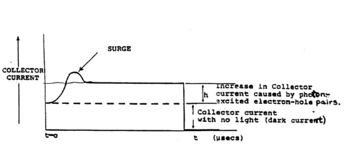
Electron-hole pairs are being generated continuously by impinging light shown at point A. In order that the distance from A, the point of generation of the minority carriers and the collector point contact 4 can be determined, the light falling on the germanium surface must be in the form of a very narrow strip of light. Under conditions when no voltage pulse is applied, these excess carriers will diffuse randomly away from the point A and recombine. Upon application of the voltage pulse, the collector becomes reverse biased and there will be an immediate surge of current appearing in the collector circuit. This is due to the collector contact attracting the holes generated prior to the application of the pulse and which have drifted along the bar without recombining under the influence of the applied pulse. Following this surge, the collector current will fall back to a constant value, but a value higher than the dark current value caused by the holes generated during the time the pulse is on. The electrons generated by the light will move in the opposite direction to the holes along with the other majority carriers. An ideal waveshape, as seen on the oscilloscope connected across RL is shown in Fig. 8.
|
Figure 8 - Oscilloscope display.
|
Procedure
- Connect the germanium sample to the supply unit through the four-pin Jones socket and attach it to the manipulator by the two screws.
- Position the cover over the sample and adjust the manipulator so that the aperture is placed over the sample approximately midway between the emitter and collector.
- Connect the oscilloscope to the oscilloscope outlets on the supply unit. Turn the contact switch to "RECT" and switch on the pulse generator. Adjust the pulse height to give approximately 30 volts and adjust the collector bias to give a suitable waveshape as indicated in section 2.2.
- Plug the light source into the two-pin socket at the side of the supply unit and mount it in a suitable stand directly above the aperture. Turn it on, and adjust its height to produce a small intense spot of light over the aperture. This should produce a waveshape similar to that shown in Fig. 8.
- Adjust the manipulator until the spot of light falls close to the collector, checking that the sample is moving perpendicular to the light source. This will increase h and move the surge current towards the leading edge of the waveshape (see Fig. 8).
- Maximize h; on the oscilloscope and assume that the light spot is now falling on the collector. Measure h. Move the collector contact away from the light source using the manipulator.
- Take a series of readings for h, the current increment due to the light for various distances (w) of the light source from the collector contact. Note that at 360º rotation of the screw on the manipulator moves the sample through 0.5 mm.
- Finally, use the oscilloscope to determine the height of the pulse used in the experiment, and measure the overall length of the germanium sample.
- Plot h vs. w on a log-linear scale. Calculate the slope and determine from it the lifetime of the minority carriers, together with an estimate of the error. Compare this value with your estimate in section 5.2.
Questions
- Discuss the waveshape obtained in the experiment.
- What important conditions are required for this experiment to succeed?
References
- R.A. Serway, C.J. Moses, C.A. Moyer, Modern Physics, Saunders 1989.
- S.T. Thornton, A. Rex, Modern Physics for Scientists and Engineers, Saunders 1993

