Main Page/PHYS 3220/Semiconductors I
Contents
Semiconductors I
Introduction
In this experiment we perform measurements on two differently doped samples of germanium to explore the conduction mechanisms in semiconductors. First the resistivity of the material is investigated by means of the current-voltage characteristic at room temperature. Next resistivity, at fixed current, is explored as a function of temperature in the range of -5 to 100 º C. In the third part the Hall effect is investigated by placing the semiconductor bar into a magnetic field.
Many references on solid-state physics exist that deal with the problem of conduction mechanisms in doped semiconductors. A good introduction to the physics needed for this experiment is given by A. Melissinos (ref. 1, chapter 3). A few of the essential concepts are reviewed in this introduction.
To understand the temperature dependence of the resistivity you must understand that two conduction mechanisms are in operation in the different temperature ranges. A perfect (pure) germanium crystal acts as an insulator. Natural impurities turn it into a poor conductor. To control the conduction process one adds impurities of a certain type. Elements with three outer electrons when added to the germanium provide hole states inside the gap near the valence band. These are excited even at low temperatures and populate the conduction band. Elements with five outer electrons also bind into the germanium crystal and easily give up their surplus electron, i.e., provide electron states close to the conduction band. One refers to the semiconductor material as being p-type or n-type doped respectively.
At low temperatures extrinsic conduction works, which is the result of impurities in the germanium providing electron and hole carriers. Above liquid nitrogen temperatures the impurity levels are all excited, i.e., saturated and an increase in temperature does not lead to an increase in transfer of these electron states to the conduction band (hole states to the valence band). Below room temperature there is only a small number of intrinsic charge carriers, i.e., transfers of valence electrons to the conduction band, since the energy gap is relatively large (about 0.7 eV; recall that at room temperature kT ≈ 0.025 eV). For high enough temperatures such that the intrinsic charge carrier mechanism dominates (but nevertheless a low-temperature approximation to the Fermi distribution is still valid) the charge carrier density dependence on temperature is given by
| (1) |
This expression can be used to express the resistivity (or voltage at constant bias current) as a function of temperature. The result will be different for both samples, since it also depends on the amount of charge carriers available. The additional quantities of interest to understand conduction are the mobility µ (defined as the proportionality constant between the average drift velocity and the applied electric field µE = vd); the conductivity (inverse of resistivity ρ) σ = 1/ρ, which relates the applied field and the current density J = σE. The conductivity is proportional to the charge carrier mobility and density (and the electron charge e): σ = n e µ . Resistivity and resistance R are related via the cross-sectional area A and the length of the sample l as ρ = R A l-1. To observe the Hall effect one places the semiconductor material into a magnetic field and measures how the Lorentz force deflects the charge carriers in a direction perpendicular to the field and the current (a voltage VH arises). This allows one to deduce not only the amount of charge carriers (at fixed T), but also which type dominates the conduction mechanism. The Hall coefficient is defined for given magnetic field strength B and generated electric Hall field Ey as
| (2) |
It provides a measure of the density of the charge carriers, since the Lorentz force depends on the drift velocity. Equating the compensating Hall field to the magnitude of the magnetic force allows us to relate the magnitude of RH to the inverse of the carrier density.
Experimental Procedure
Apparatus
Sample and Holder
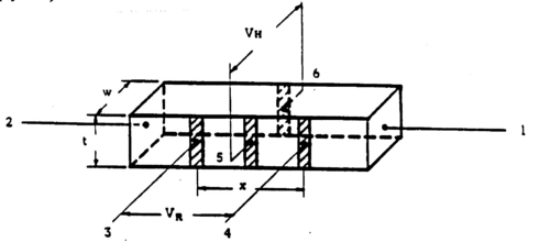
Two semiconductor samples designated RCA A and RCA B are supplied consisting of two bars of germanium (one n-type, one p-type material) mounted at the base of metal tubes. Figure 1 shows the location and function of the six contacts made to each of the samples. The samples and connections to them are visible through the plastic coating applied to protect the contacts. Understand the function of the contacts as explained in Fig. 1 and observe how the connections are realized on the two samples (contact 1 is on the sample holder side; Fig. 2 provides an explanation of current direction [engineer’s convention!] for given position of the current reversing switch on the bias supply unit).
|
Figure 1 - Contacts to the germanium samples.
|


